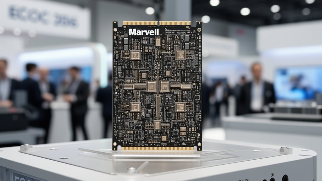
At the European Conference on Optical Communication (ECOC) 2026, Marvell Technology has officially unveiled its industry-first 2nm optical interconnect demonstrations, marking a pivotal shift in the underlying physics of artificial intelligence data centers. As hyperscalers scramble to scale next-generation AI models, the bottleneck has moved from raw compute power to the interconnects required to move data between GPUs. Marvell’s latest breakthrough is engineered specifically to address the critical power efficiency and bandwidth density requirements of architectures moving from 1.6T to 3.2T and beyond.
The 2nm Frontier in AI Infrastructure
The move to 2nm process technology is not merely a refinement of existing manufacturing capabilities; it is a fundamental shift in semiconductor physics. In the context of AI infrastructure, the 2nm node offers the ability to pack significantly more transistors into the same silicon footprint, which is essential for managing the sheer scale of modern AI clusters. Marvell’s application of this process to optical interconnects signifies that the company is tackling the ‘power-per-bit’ challenge head-on. As AI models grow to trillions of parameters, the energy consumption required for data transmission across server racks has become a primary constraint on growth. By moving to 2nm, Marvell is optimizing the physical layer, reducing the heat generated by data movement while simultaneously increasing the volume of data that can be processed per watt of electricity.
This demonstration at ECOC 2026 serves as a bellwether for the broader semiconductor industry. As current 3nm and 5nm technologies approach their thermal and density limits, the industry has been looking for a leap-frog technology that can sustain the growth of AI infrastructure. Marvell’s proactive stance on 2nm optical interconnects signals that the company is aiming to secure its role as the backbone of the next generation of data centers, providing the silicon photonics ecosystem that cloud giants like AWS, Google, and Microsoft rely upon to power their generative AI services.
The Great Leap: From 1.6T to 3.2T
The transition from 1.6T (Terabit) to 3.2T interconnect speeds is the defining engineering challenge of the mid-2020s. At 1.6T, copper-based cabling and existing silicon interposers are nearing their theoretical limits, struggling with signal attenuation and heat dissipation. Marvell’s new 2nm-based optical interconnects utilize sophisticated digital signal processing (DSP) and high-speed electro-optics that effectively bypass these physical limitations. By integrating the optical engine with the 2nm logic, Marvell is reducing the signal path distance, thereby lowering latency and improving the signal integrity required for 3.2T throughput.
This is not simply a faster connection; it is a fundamental redesign of the data center fabric. At 3.2T, a server cluster can essentially double its throughput compared to current standards without requiring a doubling of physical floor space or power infrastructure. This density efficiency is the ‘holy grail’ for data center operators. It allows hyperscalers to fit more compute power into existing facility footprints, significantly lowering the total cost of ownership (TCO) for massive AI training clusters. The demonstration at ECOC 2026 showcases that this technology is moving out of the R&D labs and into the prototype phase, ready to support the next cycle of AI hardware refreshes.
Why Silicon Photonics is the Solution
The industry has long known that electrical signals on copper traces cannot scale indefinitely. The resistance and signal loss at high frequencies become prohibitive. Silicon photonics—the technology powering Marvell’s new interconnects—uses light to transmit data rather than electricity. This approach is inherently more efficient at higher speeds. By coupling this with the 2nm process node, Marvell is addressing the two biggest costs in data centers: electricity and real estate.
Furthermore, the integration of these interconnects into the switch and GPU fabric allows for a more modular architecture. Companies can build ‘disaggregated’ data centers, where memory, compute, and networking resources are pooled rather than localized in a single server chassis. Marvell’s technology acts as the ‘nervous system’ for this disaggregated future. The ECOC 2026 demonstration specifically highlights how these 2nm interconnects maintain signal integrity over longer distances, allowing data center architects more flexibility in how they design their server racks, moving away from rigid, single-rack limitations toward fabric-wide AI supercomputers.
Future-Proofing the AI Ecosystem
Looking beyond the immediate performance gains, Marvell’s announcement at ECOC 2026 serves as a strategic roadmap for the rest of the ecosystem. Optical networking companies, packaging specialists, and hyperscalers must now align their standards and investments to accommodate these 2nm-based interconnects. As we push toward 3.2T and eventually 6.4T architectures, the standard-setting done today—and the demonstrations like the one Marvell is showcasing—will define the winners and losers of the infrastructure war. Marvell is effectively saying that the race to 2nm is won, and the next competition is on who can deploy it most reliably at scale.