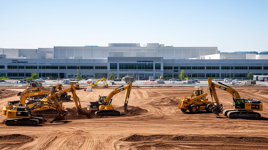
Lam Research has officially broken ground on a monumental $1.5 billion expansion project at its Tualatin, Oregon facility, marking a critical milestone in the company’s efforts to lead the semiconductor equipment market. This expansion is designed to create a specialized hub for advancing AI chip manufacturing technology, a move that underscores the company’s pivot toward addressing the explosive global demand for high-performance computing hardware. Supported by a strategic tax abatement agreement with Washington County and Tualatin municipal officials, the project serves as a cornerstone of Lam’s broader $3 billion global infrastructure initiative, signaling a massive influx of capital into the regional tech ecosystem.
Key Highlights
- $1.5 Billion Investment: A massive capital injection specifically focused on expanding the Tualatin campus’s innovation and production capacity for semiconductor equipment.
- AI-Centric Roadmap: The expansion is explicitly targeted at developing next-generation hardware required for artificial intelligence chip fabrication.
- Strategic Economic Incentives: Secured via tax abatements from Washington County and Tualatin, highlighting the importance of regional cooperation in attracting high-tech manufacturing.
- Global Scale: This project is a key component of a larger $3 billion global initiative aimed at bolstering supply chain resilience and manufacturing throughput.
Powering the AI Revolution: The Tualatin Expansion
The Strategic Shift Toward AI
For Lam Research (NASDAQ: LRCX), the Tualatin expansion is more than just a physical footprint increase; it is a tactical response to the seismic shift in global semiconductor requirements. As artificial intelligence models grow in complexity—requiring more efficient memory and processing power—the equipment needed to fabricate these chips must undergo rapid evolution. This new facility will focus on the precision engineering of tools that etch and deposit materials at the atomic level, which is essential for creating the advanced logic and memory chips that power data centers and AI accelerators.
By centralizing this work in Oregon, Lam is positioning itself at the nexus of the ‘Silicon Forest,’ a region with a deep talent pool and a long-standing infrastructure for semiconductor development. The $1.5 billion investment allows for the installation of state-of-the-art cleanroom environments, which are necessary for the development of high-NA EUV (Extreme Ultraviolet) lithography support tools and other next-generation deposition technologies.
The Anatomy of the Deal: Economic Incentives
Large-scale industrial projects of this magnitude rarely proceed without substantial public-private coordination. The tax abatement agreement reached between Lam Research and Washington County is a critical component of the project’s viability. By mitigating the high upfront costs associated with facility construction and equipment installation, the local tax incentives effectively ‘derisk’ the investment for Lam, allowing the company to accelerate its deployment schedule.
Critics often debate the long-term impact of tax abatements, but in the semiconductor sector, the competition is global. States and countries are actively bidding for manufacturing capacity; therefore, Oregon’s decision to provide a clear, stable economic environment was likely the deciding factor in keeping this specific project within the state. This agreement is not merely a tax break; it represents a commitment from the county to provide the necessary infrastructure—power, water, and specialized labor support—that a facility of this size requires to remain operational 24/7.
Scaling for a $3 Billion Vision
This Tualatin project is a primary pillar of Lam’s broader $3 billion global investment strategy. The company is simultaneously upgrading its manufacturing capabilities in other key global hubs, aiming to increase total throughput to meet the projected demand for AI-enabling chips through the remainder of the decade. This tiered approach—upgrading regional hubs while maintaining central R&D—allows Lam to be more resilient against supply chain shocks.
Integrating the Tualatin site into this global network provides Lam with a critical ‘Center of Excellence’ for its deposition and etch equipment. As the company prepares for the next cycle of semiconductor development, having this capacity online will be the difference between meeting customer timelines and falling behind in the competitive race to build the hardware that powers the AI era.
Impact on the ‘Silicon Forest’
The ripple effect of a $1.5 billion project on the local economy is substantial. Beyond the immediate construction jobs, the long-term presence of this facility ensures the retention and growth of high-skill engineering, maintenance, and facility management roles in Washington County. This expansion solidifies Tualatin’s role as an indispensable node in the global semiconductor supply chain, ensuring that Oregon remains a premier destination for tech companies looking to scale their physical operations.
FAQ: People Also Ask
How will this expansion specifically support AI technology?
The facility will focus on manufacturing advanced deposition and etching tools that are critical for building high-bandwidth memory (HBM) and next-generation logic chips, both of which are foundational to AI computing hardware.
Why was the tax abatement crucial for this project?
Semiconductor manufacturing is incredibly capital-intensive. The tax abatement lowered the immediate tax burden on the company, allowing Lam Research to prioritize capital expenditure toward specialized equipment and advanced laboratory infrastructure rather than operational overhead.
What does this project mean for the local economy?
Beyond the initial construction phase, the project ensures long-term job stability in Tualatin and Washington County, drawing in specialized engineering talent and supporting a robust ecosystem of local vendors and service providers linked to the semiconductor industry.